Scientists capture 1st-ever images of electric charges inside solar cell
What's the story
In a major scientific breakthrough, a team of researchers from the University of California Santa Barbara (UCSB) has captured the first-ever images of electric charges, moving across semiconductor materials in a solar cell.
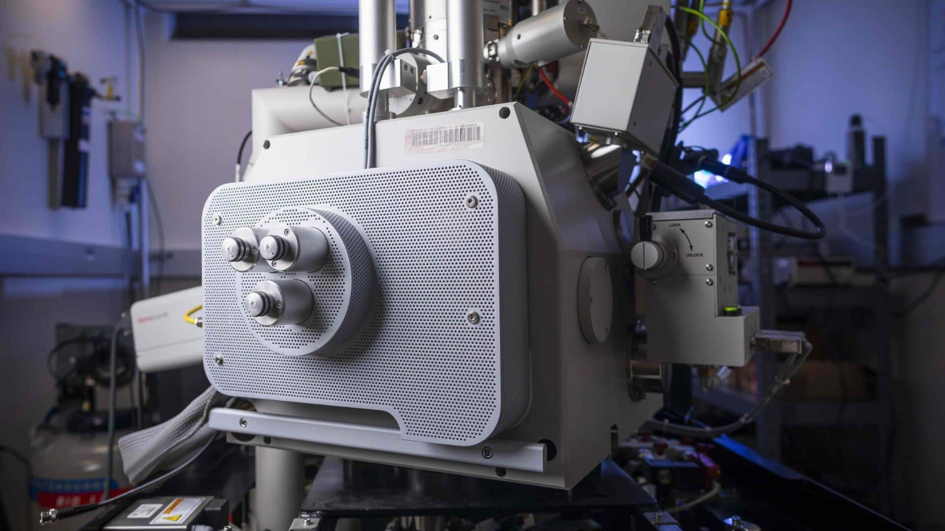
The team used a scanning ultrafast electron microscope (SUEM) for this groundbreaking research, a university press release said.
The achievement could greatly improve our understanding of semiconductor materials and their behavior.
Semiconductor behavior
Theoretical understanding of semiconductors
The behavior of semiconductor materials and the movement of charges within them, are some of the most basic concepts in science. These theories are used in everything from solar cells to computer chips.
However, a common problem with these applications is that they generate excess heat from continuous operation.
This heat release, be it powered by electricity or sunlight, is energy waste that could be reduced for improved device efficiency.
Energy conversion
Photocarriers: The key to solar cell operation
The way a solar cell works is pretty simple. Sunlight hits the semiconductor material and excites the electrons, making them move.
The movement creates a current by separating these electrons from their oppositely charged 'holes.'
The current is collected by the solar cell apparatus, while the electrons return to their holes.
These excited electrons or photocarriers lose their energy within picoseconds (10^-12), with only small fraction of this energy being captured by the solar cell, and rest released as heat.
Research approach
Visualizing photocarriers across heterojunctions
Visualizing the movement of photocarriers across heterojunctions, where electrons have to cross an interface between different materials, is difficult.
To tackle this challenge, the research team, led by Bolin Liao, an associate professor of mechanical engineering at UCSB, used ultrafast electron microscopy.
"If you excite charges in the uniform silicon or germanium regions, the hot carriers move very fast; they have a high speed initially because of their high temperature," Liao explained.
Innovative technique
Capturing the movement of electric charges
The research team employed a heterojunction of silicon and germanium for their study, because of its potential applications in solar panels and telecommunications.
To capture the image of the charges moving (which happens within picoseconds), they created a picosecond-scale shutter.
The team fired ultrafast laser pulses at the heterojunction to visualize this movement activated by an optical beam.
"What we're talking about are events happening within this picosecond to nanosecond time window," Liao said.