OpenAI to finalize 1st custom AI chip's design by year-end
What's the story
OpenAI, the company behind ChatGPT, is taking big steps to reduce its reliance on NVIDIA for chip supply.
The firm is said to be finalizing the design of its first in-house artificial intelligence (AI) silicon in the next few months, as per Reuters.
The move marks a major shift in OpenAI's strategy as it seeks to strengthen its position in negotiations with other chip suppliers.
Production plans
Chip design to be manufactured by TSMC
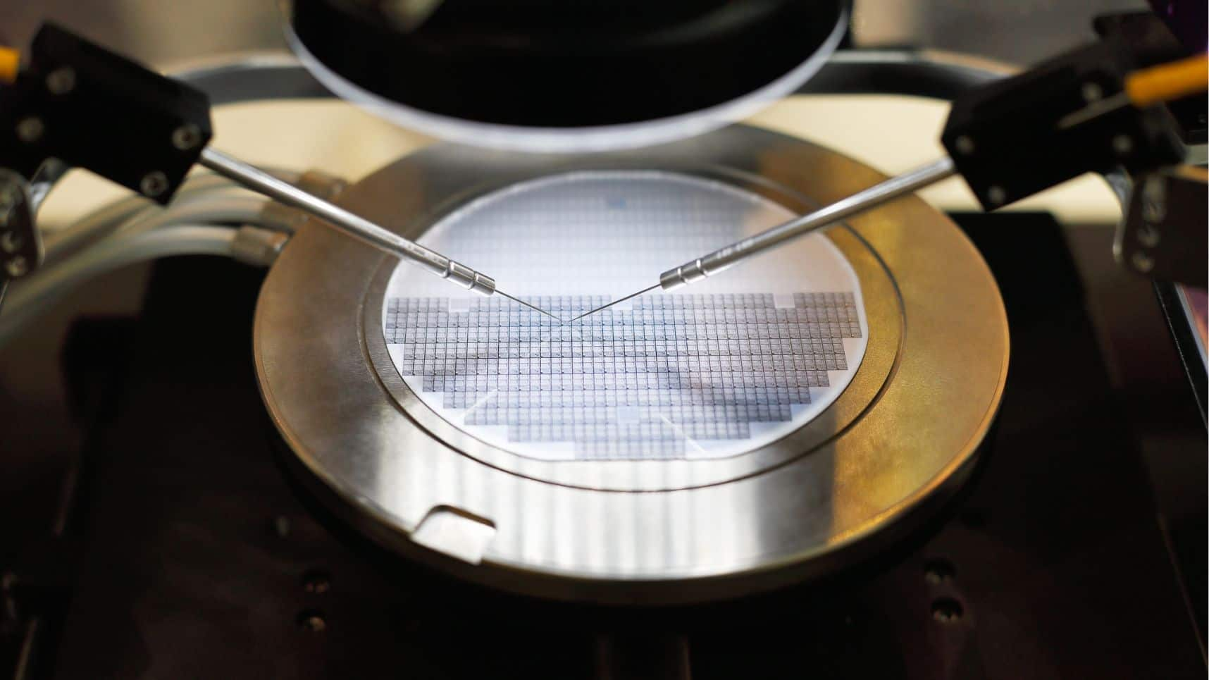
OpenAI intends to send its first in-house chip design for fabrication at Taiwan Semiconductor Manufacturing Co (TSMC).
The process, called "taping out," usually costs tens of millions of Dollars and takes around six months to yield a finished chip.
The company is on schedule for mass production at TSMC in 2026, unless it chooses expedited manufacturing at an extra cost.
Strategic tool
A strategic move
The in-house chip is viewed as a strategic weapon in OpenAI's arsenal, designed to bolster its bargaining power with other chip suppliers.
After the first chip, the company's engineers intend to develop more sophisticated processors with every new iteration.
If the first tape-out goes well, it could enable OpenAI to mass-produce its first in-house AI processor and possibly test an alternative to NVIDIA's chips later this year.
Speedy development
Rapid progress in chip design
OpenAI's plan to send its design to TSMC this year shows how quickly the firm is moving on its first design. This is a process that can take other chip designers years longer.
The processor is being designed by an in-house team at OpenAI, led by Richard Ho and supported by Broadcom.
Ho, who previously led Google's custom AI chip program, has seen his team double in size over recent months.
Chip features
OpenAI's in-house AI chip: Capabilities and limitations
OpenAI's in-house AI chip, which can train and run AI models, will be deployed on a small scale at first.
The chip is being produced by TSMC with its cutting-edge 3-nanometer technology. It uses a widely-used systolic array architecture with high-bandwidth memory (HBM) and extensive networking capabilities.
However, despite all this, the chip will play a limited role in the company's infrastructure.