8 Indian institutes launch LEAP, Rs. 40cr microscope for atoms
What's the story
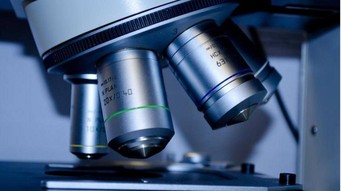
Atoms are an integral area of research for science, so eight reputed Indian institutions came together, pooled in Rs. 40cr and developed a remotely operable microscope.
Called LEAP, the "world's first of its kind" device gives a precise view of an atom, the fundamental constituent of any matter, said IIT-Madras, which spearheaded the project.
Any researcher stationed anywhere can operate LEAP through terminals.
Funds
Five IITs among eight to make it happen
Terminals for accessing the Local Electrode Atom Probe (LEAP) have been set up in all partner-institutions: IITs of Bombay, Delhi, Kanpur, Kharagpur and Ropar, ARCI and Board of Research in Nuclear Sciences (BRNS).
For the project, each contributed Rs. 2cr; BRNS gave a crore extra.
The rest was obtained through DST's 'Nano-mission' headed by CNR Rao, head of Scientific Advisory Council to the PM.
Uses
LEAP to be useful in nanotechnology, steel, automobile, energy industries
LEAP, inaugurated yesterday at the National Facility of Atom Probe Tomography (NFAPT), will contribute hugely to industries like steel, automobile, energy and various other sectors, said Prof BS Murty, Principal Investigator, NFAPT Project.
Since the high-performance microscope would enable a 3D atomic scale reconstruction, research in the field of nanotechnology will receive a big thrust, Murty added.
Worldwide, there are 100 functional LEAPs.
Details
LEAP evaporates its compound, then detects using sensor
Here's how LEAP works. Using 'Atom Probe tomography (APT)' technology, LEAP would first sharpen the compound and put it through either electroplating or an ion beam.
It is then hit with high-intensity pulsing lasers that tear the composition of the compound, breaking it into individual atoms.
The evaporated atoms can be studied through a sensor.
Finally, the data would produce a 3D visualization.
Information
What's APT, the technology to be used by LEAP?
APT has existed since 50 years, but the version to be used by LEAP was started 15 years back. The modern LEAP device would use laser pulsing methods, which will help one investigate a wide range of materials, like metals, ceramics, semiconductors and even insulators.